Article#: DGC/ART/021
The global semiconductor industry is undergoing unprecedented expansion, driven by demand from artificial intelligence, electric vehicles, telecommunications, consumer electronics, and advanced manufacturing. As nations invest heavily in semiconductor manufacturing capabilities, the challenge extends far beyond constructing buildings. Semiconductor fabrication facilities, commonly known as fabs, represent some of the most complex industrial environments ever created.
At Design Genesis Consultants Pvt. Ltd., we believe that the success of a semiconductor facility begins long before detailed engineering. It starts with strategic master planning that integrates infrastructure, manufacturing requirements, utility resilience, sustainability, and future scalability into a unified development vision.
Why Semiconductor Facilities Demand Specialized Planning
Unlike conventional manufacturing plants, semiconductor factories operate within highly controlled environments were microscopic contamination, utility interruptions, or environmental fluctuations can significantly impact production quality.
A semiconductor fab functions as a sophisticated ecosystem comprising:
- Cleanroom facilities
- Advanced process equipment
- Ultra-pure water systems
- High-capacity electrical infrastructure
- Specialty gas distribution networks
- HVAC and environmental control systems
- Chemical handling facilities
- Waste treatment infrastructure
- Logistics and warehousing zones
The interdependence of these systems makes master planning a critical success factor.
Site Selection: The Foundation of Success
The first step in semiconductor facility planning is selecting the right location.
Several factors influence site suitability:
Infrastructure Availability
Semiconductor plants require reliable access to:
- High-capacity electrical power
- Redundant utility networks
- Water resources
- Transportation connectivity
- Telecommunication infrastructure
A disruption in any of these systems can lead to significant production losses.
Geotechnical and Environmental Considerations
Site evaluation must assess:
- Soil conditions
- Seismic activity
- Flood risk
- Environmental sensitivities
- Groundwater characteristics
- Climate conditions
Early identification of site constraints reduces future development risks and capital expenditure.
Master Planning for Efficient Manufacturing Operations
An effective semiconductor campus is planned around operational efficiency.
The arrangement of production buildings, utility infrastructure, logistics corridors, and support facilities directly influences productivity and future expansion opportunities.
Process-Centric Layout Planning
Manufacturing workflows should drive the master plan.
Key objectives include:
- Optimizing material movement
- Reducing transportation distances
- Minimizing process disruptions
- Improving operational accessibility
- Supporting automation systems
Well-planned layouts improve productivity while reducing operational costs.
Utility-Centric Planning
Utilities are the backbone of semiconductor manufacturing.
Master planning must accommodate:
- Substations and power distribution systems
- Backup generation facilities
- Chilled water networks
- Compressed air systems
- Ultra-pure water plants
- Wastewater treatment facilities
- Specialty gas storage and distribution
These systems require careful zoning to balance operational efficiency, safety, and maintainability.
Cleanroom Planning: The Heart of Semiconductor Manufacturing
Cleanrooms represent the most critical and technically demanding component of a semiconductor facility.
Master planning considerations include:
Environmental Control
Cleanrooms require strict management of:
- Air quality
- Temperature control
- Humidity regulation
- Particle contamination
- Air pressure differentials
Even minor environmental deviations can impact yield rates and product quality.
Semiconductor equipment often imposes stringent structural requirements, including:
- Vibration control
- Long-span floor systems
- High load-bearing capacities
- Precise floor flatness tolerances
These requirements must be integrated into the facility design from the earliest planning stages.
Building for Scalability and Future Growth
Semiconductor technology evolves rapidly. Facilities designed solely for immediate production needs often face operational constraints within a few years.
A forward-looking master plan should accommodate:
- Capacity expansion
- Technology upgrades
- Additional production lines
- Increased utility demands
- New process technologies
Future-ready planning reduces disruption and allows organizations to respond quickly to changing market demands.
Sustainability in Semiconductor Facility Design
Despite their high utility demands, modern semiconductor factories increasingly prioritize sustainable design and resource efficiency.
Key sustainability strategies include:
Water Management
Given the substantial water requirements for semiconductor manufacturing, facilities should incorporate:
- Water recycling systems
- Rainwater harvesting
- Advanced treatment technologies
- Water-use optimization programs
Energy Efficiency
Opportunities include:
- High-performance building envelopes
- Energy-efficient HVAC systems
- Smart building management systems
- Renewable energy integration
- Waste heat recovery solutions
Sustainable infrastructure not only reduces environmental impact but also enhances long-term operational resilience.
Risk Management Through Master Planning
Large-scale semiconductor investments involve significant financial and operational risks.
Strategic master planning helps mitigate risks associated with:
- Utility interruptions
- Regulatory compliance
- Environmental challenges
- Construction constraints
- Future expansion limitations
- Operational inefficiencies
By addressing these considerations during the planning phase, developers can improve project certainty and optimize investment returns.
Digital Engineering and BIM Integration
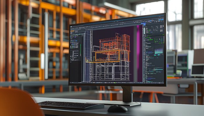
Given the complexity of semiconductor facilities, digital engineering tools have become essential.
Building Information Modeling (BIM) enables:
- Multidisciplinary coordination
- Clash detection
- Construction sequencing analysis
- Utility integration planning
- Asset lifecycle management
A digitally coordinated planning process improves design quality while minimizing project execution risks.
The Design Genesis Approach
At Design Genesis Consultants Pvt. Ltd., we approach semiconductor developments through a comprehensive master planning framework that integrates engineering, infrastructure, architecture, sustainability, risk assessment, and future scalability.
Our multidisciplinary approach ensures that manufacturing objectives, utility networks, environmental requirements, and long-term business goals are aligned from the earliest stages of development. By combining strategic planning with advanced design methodologies, we help create industrial ecosystems capable of supporting next-generation semiconductor manufacturing.
Conclusion
Semiconductor facilities are among the most sophisticated industrial developments in the modern world. Their success depends not only on advanced manufacturing technology but also on the quality of planning that precedes construction.
A well-executed master plan establishes the foundation for operational efficiency, utility reliability, environmental sustainability, and long-term growth. As the semiconductor industry continues to expand globally, strategic master planning will remain a defining factor in creating resilient, future-ready manufacturing campuses.
For organizations investing in semiconductor manufacturing, thoughtful planning today is the key to technological leadership tomorrow.